 18.11.2018., 20:52
|
#4889
|
|
McG
Datum registracije: Feb 2014
Lokacija: Varaždin
Postovi: 6,773
|
AMD Discloses Initial Zen 2 Details
Citiraj:
AMD evaluated both 10 nm and 7 nm. The choice to go with 7 nm boiled down to the much lower power and higher density they were able get. AMD has made a large set of enhancements to Zen 2. The majority of the changes to the back-end involve the floating-point units. In Zen 2, the data path is now 256 bits. Additionally, the execution units are now 256-bit wide as well, meaning 256-bit AVX operations no longer need to be cracked into two 128-bit micro-ops per instruction. With 2 256-bit FMAs, Zen 2 is capable of 16 FLOPS/cycle, matching that of Intel’s Skylake client core.
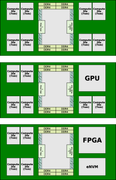
With Rome, AMD is taking the idea of chiplets further. Similar to what they initially started with Threadripper 2, Rome has compute dies and an I/O die. In total, there are nine dies. One I/O die and eight compute dies – each with 8 Zen 2 cores. The package is organized in four pairs of compute dies similar to our diagram below. It’s worth noting that each pair of compute dies are packaged tightly together on the organic substrate, indicating there might be very short traces going between them. There is a lot of mystery surrounding the capabilities of the I/O die and AMD’s plan for the future. By moving all the “redundant components”, such as the I/O and southbridge, from the compute die to the I/O die, AMD has opened up their design to some intriguing possibilities. Since all the controls can be found in the centralized I/O die, it becomes possible to swap out the compute dies with other types of logic such an FPGA (e.g., from Xilinx) or a GPU.
|
Citiraj:
|
For each 64-core "Rome" processor, there are a total of 8 chiplets. With SANDRA detecting "16 x 16 MB L3" for 64-core "Rome," it becomes highly likely that each of the 8-core chiplets features two 16 MB L3 cache slices, and that its 8 cores are split into two quad-core CCX units with 16 MB L3 cache, each. This doubling in L3 cache per CCX could help the processors cushion data transfers between the chiplet and the I/O die better. This becomes particularly important since the I/O die controls memory with its monolithic 8-channel DDR4 memory controller.
|
Izvor: WikiChip Fuse i TechPowerUp
Zadnje izmijenjeno od: The Exiled. 26.11.2018. u 08:11.
|

|

|