 07.04.2019., 19:04
|
#5406
|
|
McG
Datum registracije: Feb 2014
Lokacija: Varaždin
Postovi: 8,308
|
TSMC makes progress on 5nm with complete infrastructure design and risk production
Citiraj:
TSMC has announced that it has completed infrastructure design on its 5nm process node that will leverage the company's second generation of extreme ultraviolet (EUV), as well as deep ultraviolet (DUV) lithography. TSMC's 5nm chips will be aimed at SoC designs, 5G mobile applications, AI, and high performance computing. TSMC has also completed development of its 5nm Design Rule Manual (DRM), SPICE model (simulation program with integrated circuit emphasis), and process design kits (PDK). The entirety of the 5nm design infrastructure is available for TSMC customers via TSMC Online. TSMC also notes it has chips in risk production with its alpha customers, which likely indicates volume production could ramp in 2020. That would align with TSMC's previous plans to hit 5nm by 2020 and 3nm by 2022. Their 5 nm node continues to use bulk silicon FinFET transistors. Leveraging their experience from 7nm+, 5nm is expected to utilize EUV for more critical layers in order to reduce the multi-patterning complexity. The 5nm node is expected to deliver a 15% improvement in performance at constant power or a 20% reduction in power at constant performance. TSMC is targeting both low-power mobile and high-performance compute with this node.
|
Why AMD EPYC Rome 2P will have 128-160 PCIe Gen4 lanes and a bonus
Citiraj:
With AMD EPYC “Rome”, there are two I/O die with x86 cores that hang off the I/O die. When we look externally, AMD has a set number of pins that need to carry data to and from the socket. That includes pins for eight memory channels along with eight x16 links. We are going to leave the memory channels alone, and discuss the x16 links. With AMD EPYC 7002 or “Rome” already has PCIe Gen4 support announced, while the 2nd Gen Intel Xeon Scalable CPUs still use 14nm and Intel’s PCIe Gen3 IP. In a single socket, that means that AMD EPYC Rome will have 128 PCIe lanes using eight x16 links for PCIe. We expect AMD will use the Rome generation to add another PCIe lane, making 129 PCIe lanes total, and we are going to discuss that in our “Bonus Lanes” section later. Unlike Intel’s PCH, AMD’s chips are designed to have all I/O on package. When looking at 1st and 2nd Gen Intel Xeon Scalable systems versus AMD EPYC, one has to remember that Intel systems include a Lewisburg PCH that uses power and adds cost. AMD had a goal of using flexible I/O and its Server Controller Hub (SCH) to remove the need for the PCH.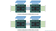 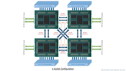
|
Izvor: TechSpot, TechPowerUp, WikiChip, RetiredEngineer i ServeTheHome
|

|

|