 22.03.2019., 21:18
|
#5342
|
|
McG
Datum registracije: Feb 2014
Lokacija: Varaždin
Postovi: 8,336
|
AMD Ryzen 3000 "Zen 2" BIOS analysis reveals new options for Overclocking & Tweaking
Citiraj:
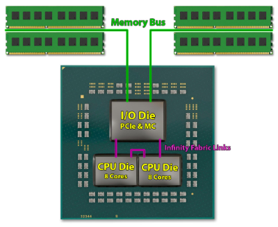
At CES 2019, AMD unveiled more technical details and a prototype of a 3rd generation Ryzen socket AM4 processor. The company confirmed that it will implement a multi-chip module (MCM) design even for their mainstream-desktop processor, in which it will use one or two 7 nm "Zen 2" CPU core chiplets, which talk to a 14 nm I/O controller die over Infinity Fabric. The two biggest components of the IO die are the PCI-Express root complex, and the all-important dual-channel DDR4 memory controller. We bring you never before reported details of this memory controller. The 3rd generation Ryzen processor (and all other Zen 2 CPUs), hence have an "integrated-discrete" memory controller. The memory controller is physically located inside the processor, but is not on the same piece of silicon as the CPU cores. AMD isn't the first to come up with such a contraption. Intel's 1st generation Core "Clarkdale" processor took a similar route, with CPU cores on a 32 nm die, and the memory controller plus an integrated GPU on a separate 45 nm die.
Intel used its Quick Path Interconnect (QPI), which was cutting-edge at the time. AMD is tapping into Infinity Fabric, its latest high-bandwidth scalable interconnect that's heavily implemented on "Zen" and "Vega" product lines. We have learned that with "Matisse," AMD will be introducing a new version of Infinity Fabric that offers twice the bandwidth compared to the first generation, or up to 100 GB/s. AMD needs this because a single I/O controller die must now interface with up to two 8-core CPU dies, and up to 64 cores in their "EPYC" server line SKU.
AMD has changed the CBS section title from "Zen Common Options" to "Valhalla Common Options." We have seen this codename on the web quite a bit over the past few days, associated with "Zen 2." We have learned that "Valhalla" could be the codename of the platform consisting of a 3rd generation Ryzen "Matisse" AM4 processor and its companion AMD 500-series chipset based motherboard, specifically the successor to X470 which is being developed in-house by AMD as opposed to sourcing from ASMedia. Unlike earlier generations, the new BIOS offers UCLK options for "Auto", "UCLK==MEMCLK" and "UCLK==MEMCLK/2". The last option is new and will come in handy when overclocking your memory, to achieve stability, but at the cost of some Infinity Fabric bandwidth.
The "Matisse" processor will also provide users with finer control over active cores. Since the AM4 package has two 8-core chiplets, you will have the option to disable an entire chiplet, or adjust the core-count in decrements of 2, since each 8-core chiplet consists of two 4-core CCX (compute complexes), much like existing AMD designs. At the chiplet-level you can dial down core counts from 4+4 to 3+3, 2+2, and 1+1, but never asymmetrically, such as 4+0 (which was possible on first-generation Zen). AMD is synchronizing CCX core counts for optimal utilization of L3 cache and memory access. For the 64-core Threadripper that has eight 8-core chiplets, you will be able to disable chiplets as long as you have at least two chiplets enabled.
|
Izvor: TechPowerUp
|

|

|